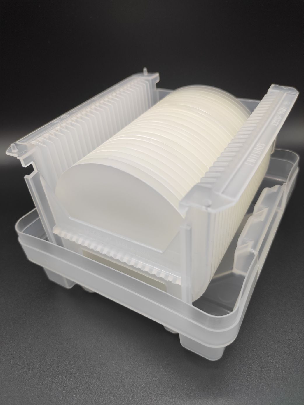
We provide Semiconductor wafers and crystals from the top high quality vendors. They are the indispensable materials for today’s civilization that drives almost all technologies to make the life easier the life for human being. LEDs, Laser diodes, detectors, sensors, transistors and Integrated Circuits, solar cells and many other semiconductor, thin film and MEMS devices are uses these substrates as a base material. There are many semicondcutor crystal growth method that helps to make those devices for our lives. Czochralski Pullers, MOCVD, MBE, HVPE, LPE, Float Zone, VGF and some other well known methods and tools are well developed to make such crystals and well established processing methods are available to make thin slice of those crystals so called wafers. From almost zero bandgap energy to high bandgap up to 6.2eV wafer materials are giving us wide spectrum of application area.
Click on the below items to see major product properties!
Contact sales@corecrystal.com for detailed technical properties of the substrate products.
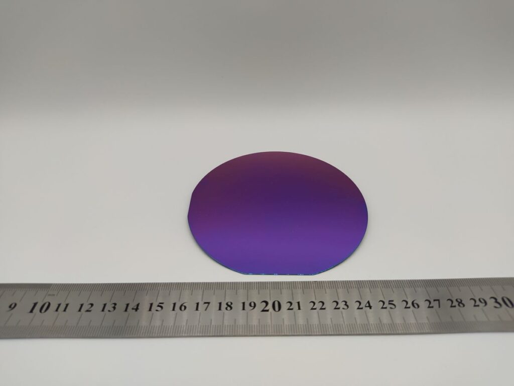
Polytype: 4H,6H
Diameter: 2″,3″,4″,6″
Conductivity: N-type, Semi Insulating
Surface Finish: Epi-Ready, Optical Polish, Fine ground, Single Side Polished, Double Side Polished
Surface Orientation: C-plane, R-plane, A-Plane
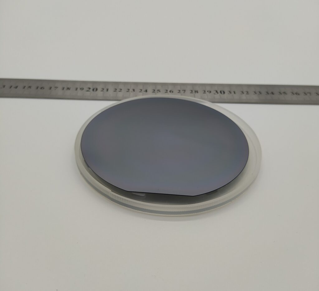
Diameter: 2″,3″,4″,6″
Conductivity: N-type, Semi Insulating
Surface Finish: PSS, Epi-Ready, Optical Polish, Fine ground, Single Side Polished, Double Side Polished
Surface Orientation: (100)
Diameter: 2″,3″,4″,5″,6″
Conductivity: N-type, P-type, Undoped
Surface Finish: Epi-Ready,Etched, Single Side Polished, Double Side Polished
Surface Orientation: (100)
Diameter: 2″,3″,4″,6″
Conductivity: N-type, P-type, Semi Insulating
Surface Finish: Epi-Ready, Etched, Single Side Polished, Double Side Polished
Surface Orientation: (100)
Diameter: 2″,3″,4″,6″
Conductivity: N-type, P-type
Surface Finish: Epi-Ready, Etched, Single Side Polished, Double Side Polished
Surface Orientation: (100), (111)
Diameter: 2″,3″
Conductivity: N-type, P-type, Semi Insulating
Surface Finish: Single Side Polished, Double Side Polished
Surface Orientation: (100), (111), (110)
Diameter: 2″,3″,4″,6″,8″
Conductivity: N-type, P-type, Semi Insulating
Surface Finish: Single Side Polished, Double Side Polished
Handle Thickness: 0.2-1.1mm
Diameter: 4″,5″,6″,8″
Handle Conductivity: N-type, P-type
Buried Oxide: 0.2µm to 15µm
Device Layer: 0.1µm to 200µm
Backside Surface: Lapped/Etched or Polished
Substrate: p type Silicon <100>
Diameter: 150mm
Thickness: 1000µm
Thermal Oxide: 0.2µm to 20µm
Free Standing GaN
Surface Orientation: <001> C-Plane
Diameter: 2″ (50mm), 4″ (100mm)
Thickness: 350µm (2″), 480µm (4″)
Conductivity: N-type, Undoped
Surface Finish: Epi-Ready, Fine ground
FWHM: < 120 arc sec
Free Standing AlN
Surface Orientation: <001> C-Plane
Diameter: 1″, 2″,3″, 4″ OR Customized Sizes
Thickness: 400µm to 1000µm
Conductivity: N-type, Undoped
Surface Finish: Epi-ready, SSP, DSP
Free Standing CZT
Surface Orientation: <111>
Size: 25mm x 25mm
Thickness: 1200µm
Zn: %3.5<x<%4.5
Surface Finish: Epi-ready

We will be happy to help you for your standart and customized semiconductor wafer needs. Contact our Expert for your research and production aiming semiconductor wafer needs.